- Switches and Sensors
- Metal Oxide Transistors
- Resistive Memory
- Printed MEMs
- Field Emission Devices
- Energy Devices
- Printed Batteries
- Flow Batteries
- Perovskite Solar Cells
- Printing and Material Development
- Gravure Printing
- Nanoparticle Inks
- Bioelectronic Interfaces
- Accelerated Lifetime Testing
Switches and Sensors
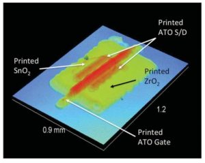
Metal Oxide Transistors
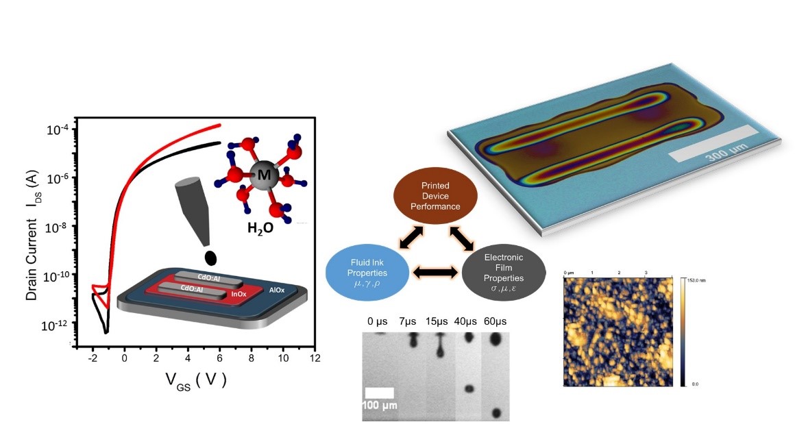
Metal oxide transistors hold great promise for a variety of applications in information display and ubiquitous sensing. Our group is developing new materials, processing, and printing methods to boost the performance of metal oxide transistors and reduce the thermal budget to enable applications on plastic substrates. We are also exploring applications of metal oxide transistors to low-power gas sensing.
Resistive Memory
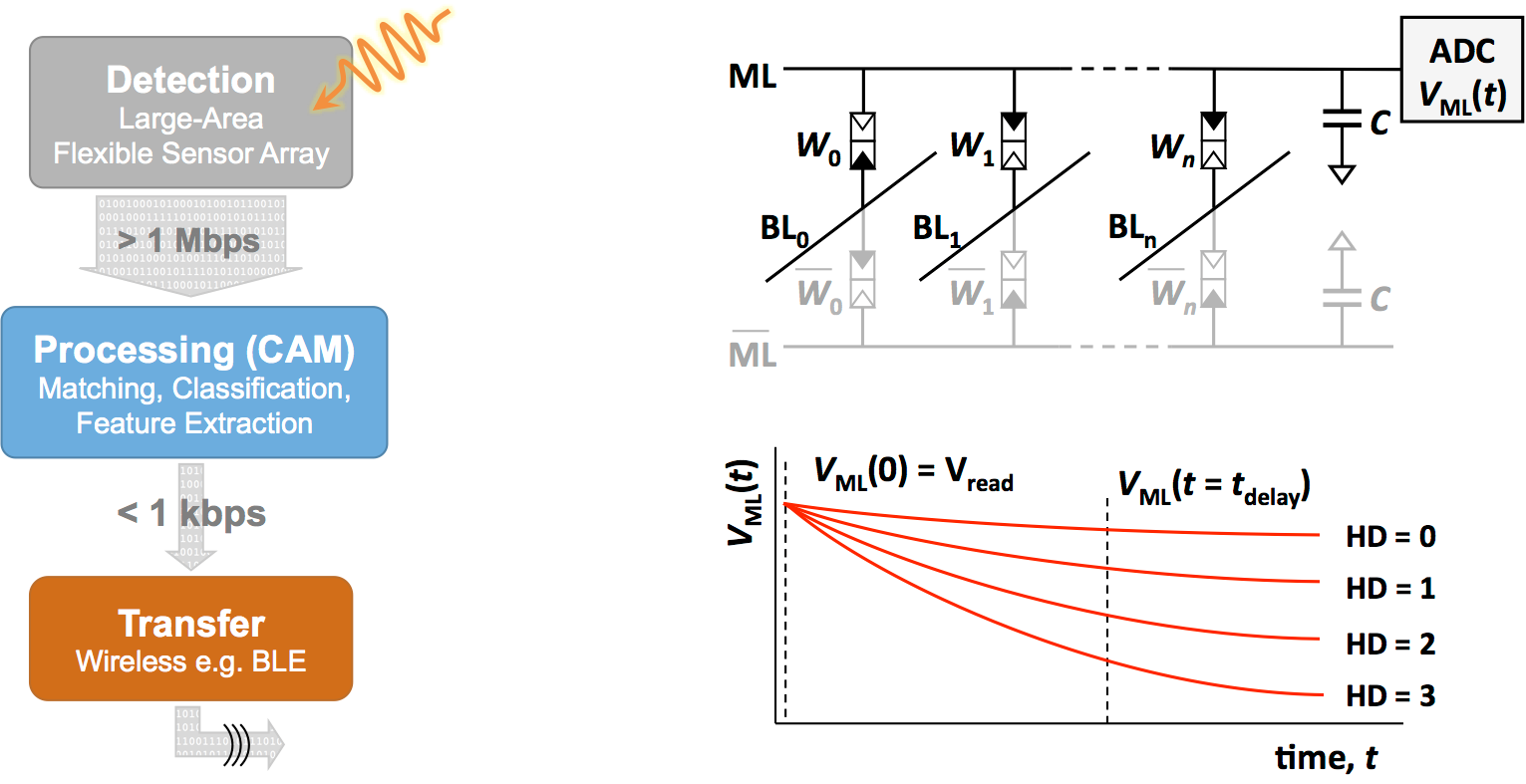
The field of resistive switching for nonvolatile memory applications has been widely researched due to its potential for low power consumption, high density of devices, simple architecture, and fast switching speed. Resistive Random Access Memory (RRAM) commonly employs transition metal oxides such as Ta2O5, NiO, TiO2, HfO2, and ZrO2 as the dielectric material in a metal–insulator–metal (MIM) geometry. To utilize such devices in an addressable memory array, complementary resistive switching (CRS) using two back-to-back RRAM elements has been demonstrated to prevent current sneak paths between memory locations. This type of structure can simplify the memory architecture by reducing the number of unique materials that have to be deposited, which is especially desirable in the case of printed electronics. However, more importantly, it also results in extremely interesting nonlinear switching behavior that can be utilized for nontraditional computing such as mimicking synaptic and multilevel behavior, stateful logic, or associative memory. This last application is particularly interesting for large-area electronics since, in conjunction with proposed applications of such systems in sensors, associated memories may enable robust pattern matching for sensor output identification.
Publication: Smith et. al. IEEE TED, 2017, PP, 99.
Printed MEMS
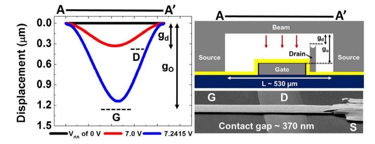
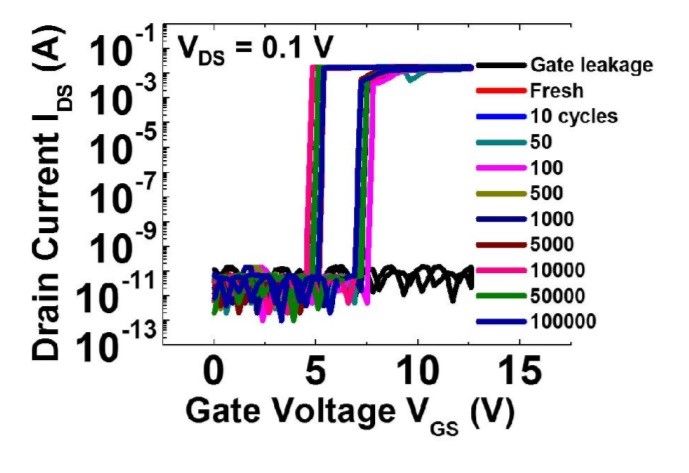
Microelectromechanical devices are essential devices in microelectronics for sensing and actuation which utilize the mechanical action of microfabricated structures. Our group has been developing fully-printed MEM switches for high-current switching. These printed MEM relays have free-standing metal beams printed from metal nanoparticle inks which are electrostatically actuated by printed gate electrodes. These devices exhibit abrupt switching of high-current loads ( > 400 mA) with extremely low-leakage in the off-state (< pA) and small mechanical delays. Our current work involves applying these printed switches to active solar bypass systems for improving performance of solar arrays under partial shading.
Field Emission Devices
Vacuum nanoelectronic devices based on field emission present an exciting new area of research that combines the superior technical performance of vacuum-based devices with the microfabrication ease of solid-state technology. In the present work, we are developing and characterizing microfabricated
Energy Devices
Printed Batteries
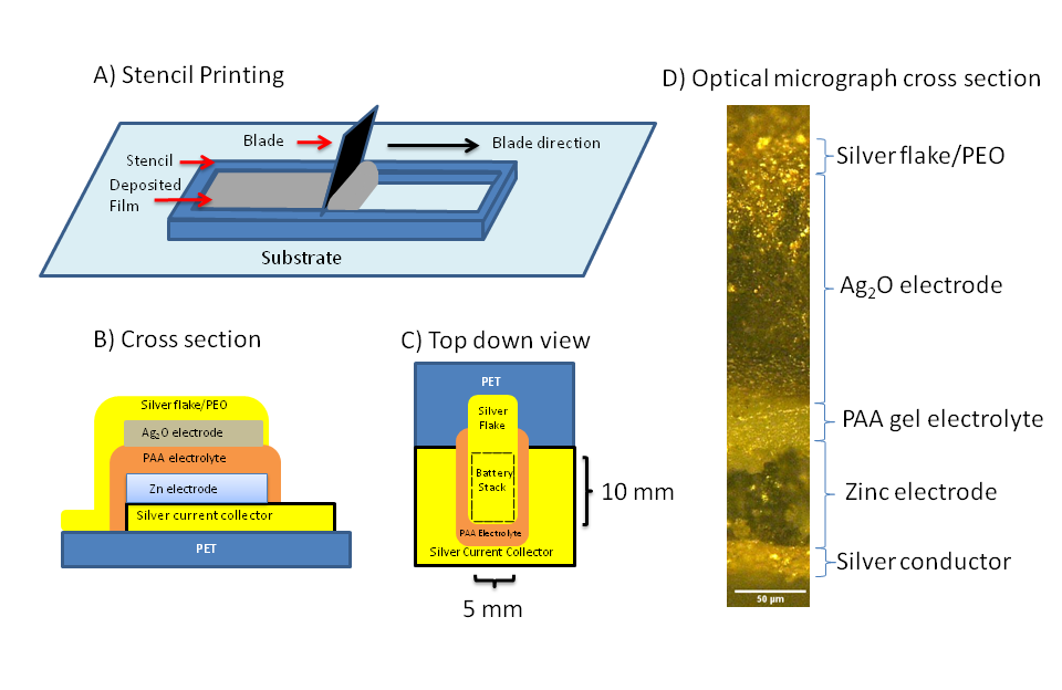
Printed batteries are an emerging energy storage technology, providing on-device power sources for wireless and flexible electronics applications. While partially printed battery systems have been demonstrated, fully printed batteries would enable seamless additive manufacturing of integrated systems such as wearable electronics or printed radio-frequency identification (RFID) tags.
Previously, we have demonstrated a printed silver-oxide battery using a novel photopolymerizable sol-gel electrolyte and separator. Currently, our group has continued work on the silver-oxide battery system and made progress in electrode ink design, mitigating battery degradation mechanisms, and scaling batteries for device integration. In addition, we have begun work on a printed Zn-air battery for high energy density applications.
Publications: Braam et. al. Adv. Mater. 2015, 27, 4.
Flow Batteries
Redox flow batteries (RFBs) are a highly efficient energy storage technology that relies on the redox states of electrochemical systems for conversion of chemical to electrical energy. While conventional batteries store energy in solid electrodes, RFBs store energy externally and are only introduced into the device during operation. This allows power and energy to optimized independently, making RFBs uniquely capable of serving a wide variety of application. Currently, our group has focused on two emerging areas of RFBs: microfluidic and semi-solid flow batteries.
Perovskite Solar Cells
Perovskite solar cell research has been at the forefront of the photovoltaic community for the past few years. Many different formulations of the perovskite structure have resulted in relatively high power conversion efficiencies, which are currently comparable to single junction crystalline silicon solar cells. However, there are three main areas that remain an issue moving forward with perovskites: (1) Stability in atmospheric conditions, (2) Toxicity due to the presence of lead in most “stable” and efficient formulations, and (3) High scale processing for large area processing to make perovskite solar cells commercially viable. We seek here to get a better understanding of the intrinsic processes in perovskites and leverage those to manufacture better cells.
Printing and Material Development
Gravure-Printing
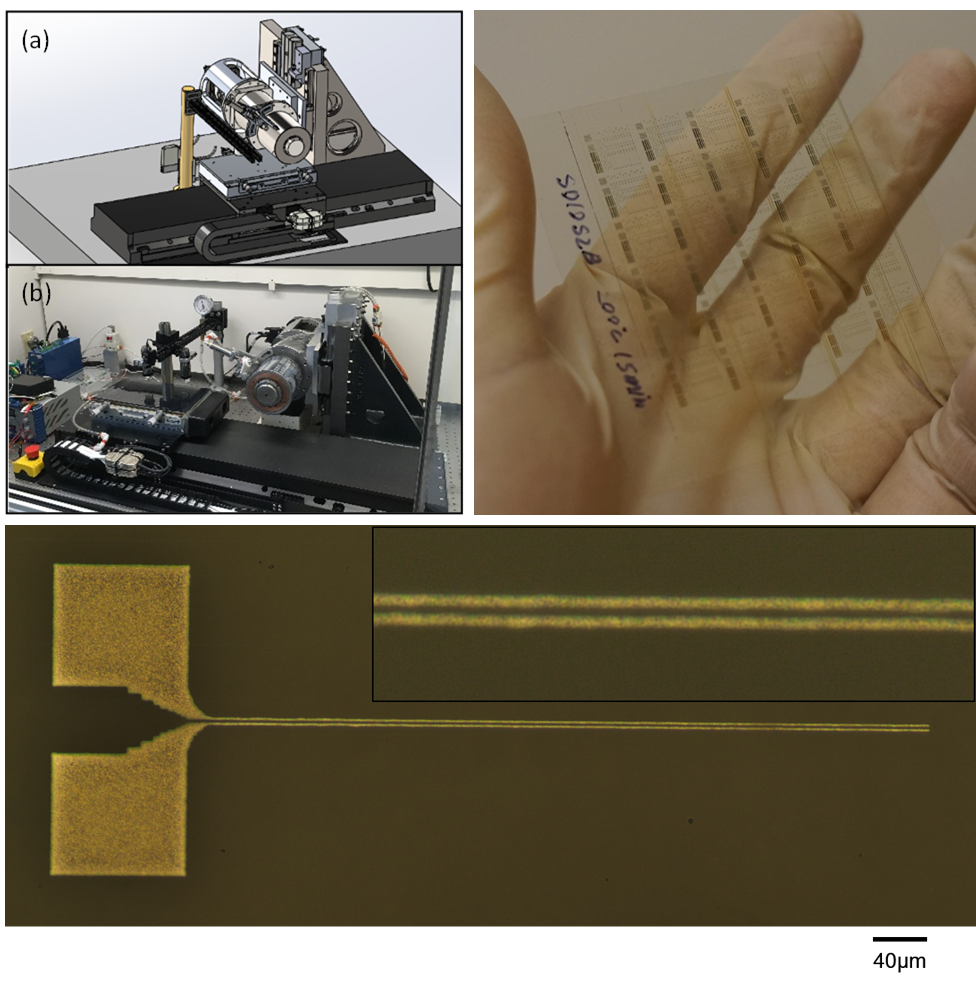
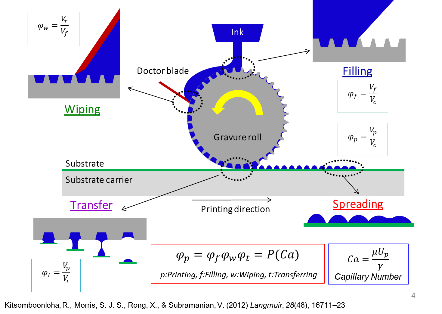
Among many techniques for printed electronics, gravure printing offers superior resolution (< 5 µm) and high throughput (> 1 m/s) –advantages that make it an industrially proven, high-volume manufacturing technology used in the graphic arts. We have worked to understand the governing fluid mechanics of gravure printing, design 0D and 1D nanomaterial inks to enable printing of high-quality devices, and develop new tools and processes for high-speed patterning. Recently, we applied that knowledge about the physics of gravure printing to design and construct a laboratory scale sheet-fed gravure printer for high-speed nanomaterial printing with high registration accuracy. By decoupling each of the subprocesses of gravure, we have also been able to develop a greater understanding of the ink transfer, doctoring, and filling of nanomaterial inks. This understanding has allowed us to scale the critical dimension of gravure-printed lines to below 2 µm.
Nanoparticle Inks
In this project, we are developing metallic nanoparticles for use in printed conductor applications. We have developed a range of particles, including gold, silver, and copper, and are applying them to a broad spectrum of applications in printed electronics, semiconductor packaging, and photovoltaic applications. As part of this work, we have developed novel synthetic strategies for forming high-quality nanoparticles.
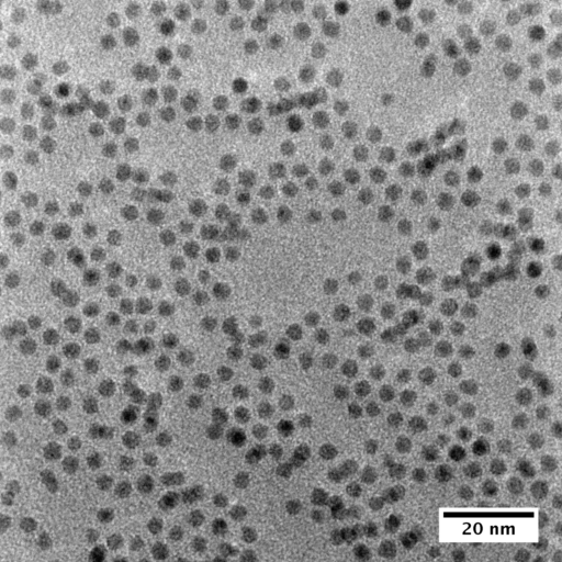
We have performed detailed mechanistic studies on the sintering of nanoparticles.

Figure 1 : Summary of crystallite size derived from XRD data for films annealed in air and N2.
Using the above knowledge, we have fabricated a wide range of devices and structures, including transistors, passive components, PV bus bars, and interconnects.
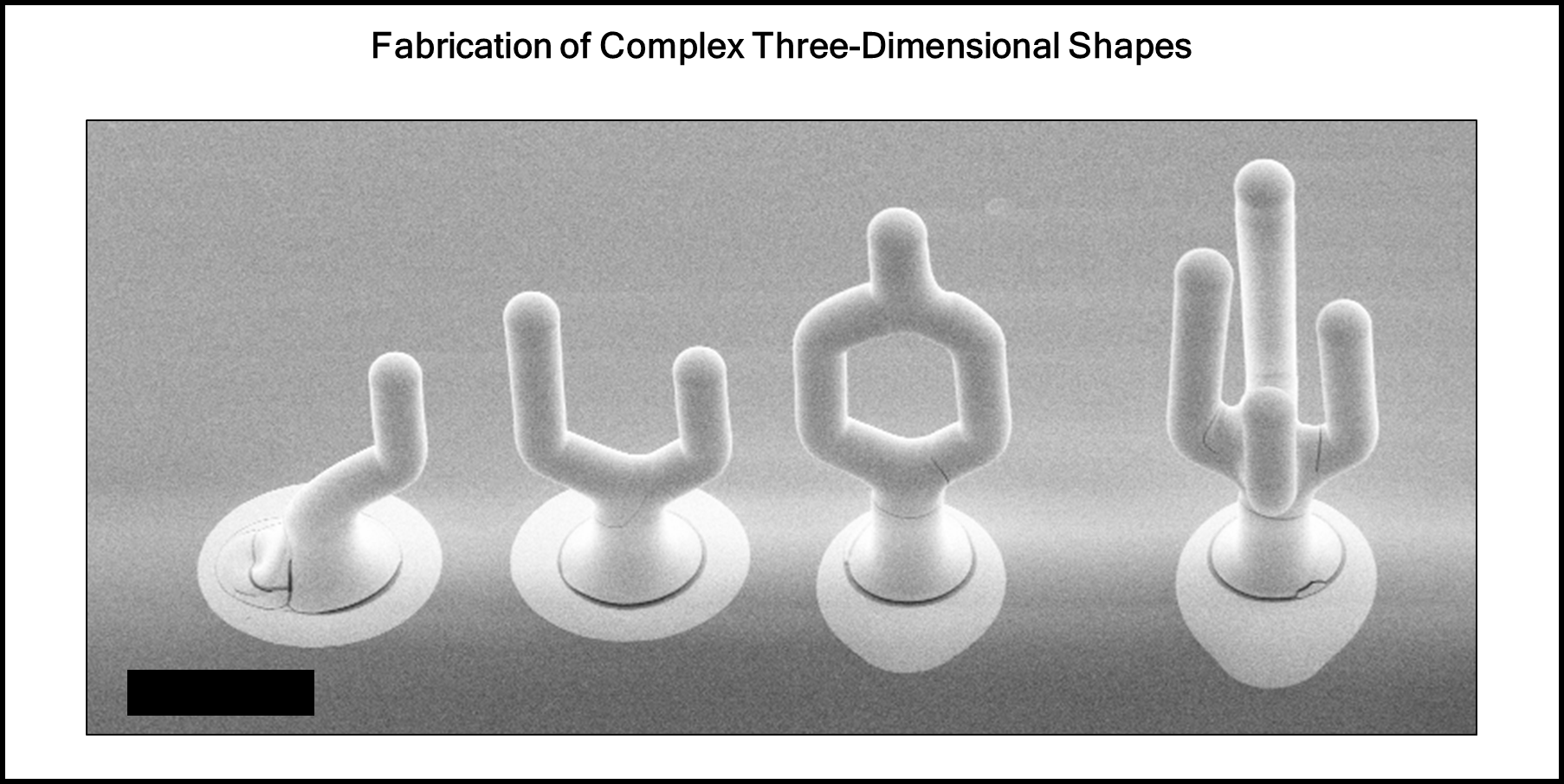
Figure 2 : Complex three-dimensional shapes fabricated using principles learned from simple freestanding pillar fabrication. Scale bar represents 200 µm.
Bioelectronic Interfaces
Accelerated Lifetime Testing
Aging of Biological Implants Project: Neurological implants have great potential for treating brain disorders as well as interfacing with artificial limbs. In order to be a viable treatment option, these implants are expected to perform for ten to fifteen years. Unfortunately, most of these devices fail within the first few months or years. The goal of this project is to identify the root causes of these failures more precisely and use biological acceleration to predict the lifetime of devices in an acceptable timeframe. By using a combination of both chemical, thermal, and biological attack, our group hopes to better represent the degradation environment of the human brain.

